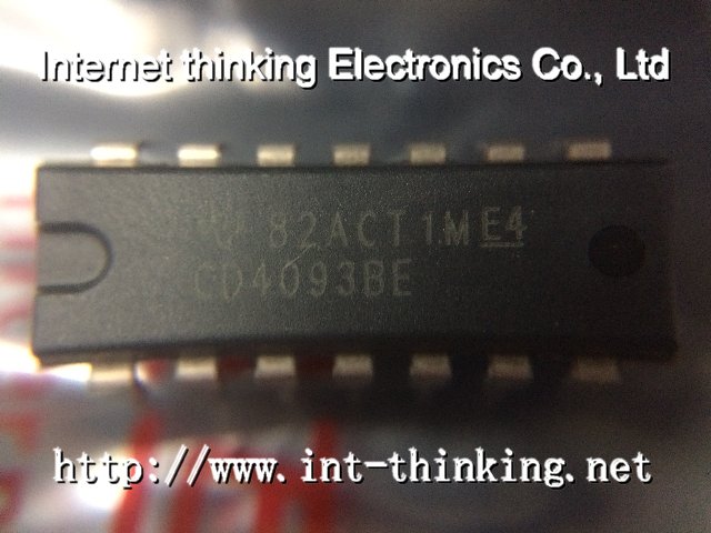
CD4093B consists of four Schmitt-trigger circuits. Each circuit functions as a two-input NAND gate with Schmitt-trigger action on both inputs. The gate switches at different points for positive- and negative-going signals. The difference between the positive voltage (VP) and the negative voltage (VN) is defined as hysteresis voltage (VH) (see Fig. 2).
The CD4093B types are supplied in 14-lead hermetic dual-in-line ceramic packages (F3A suffix), 14-lead dual-in-line plastic packages (E suffix), 14-lead small-outline packages (M, MT, M96, and NSR suffixes), and 14-lead thin shrink small-outline packages (PW and PWR suffixes).


 | 2 訂單數量
 --->>>到達時間 5-7天
 --->>>到達時間 15-27天
 --->>>到達時間 5-7天
 規格書
規格書


 吴*****

